- Contact 0870 350 7767
- |
- Advertise

How to reduce the costs of fine-line PCBs
 News and PR from Eurocircuits - Published 29 April 2016
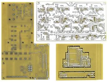
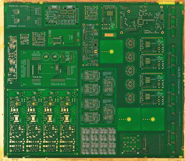
Our customers regularly call us to say that they have laid out a PCB with fine-pitch BGAs.
News and PR from Eurocircuits - Published 29 April 2016
Our customers regularly call us to say that they have laid out a PCB with fine-pitch BGAs. Our customers regularly call us to say that they have laid out a PCB with fine-pitch BGAs. The layout looked OK in EAGLE, but when they uploaded the data onto our website they got a message that there were too many DRC errors so we couldnÂt produce the board, or, if we could, only at a higher price.
What has gone wrong?
Most designers start their layout using the PCB manufacturerÂs standard specification for the smallest standard track and isolation widths and the smallest drill sizes. For Eurocircuits these are:
Example:
- 150 µm Track/Gap and 0,25mm Drill End-diameter
- Or for a small but affordable extra charge 125 µm Track/Gap und 0,15 Drill End-diameter
So the designer typically uses the smallest standard drill size, 0.25 mm, for the via holes, routes the tracks in accordance with the standard DRC values and makes sure that tracks are centered between pads.
The results on screen looks OK. So the designer uploads his data right away into the online data checker, PCB Visualizer, but then he finds that there are errors everywhere. He can start to work his way through the list but will soon find that it is nearly impossible to solve all errors. The only solution is to change to a more expensive service.
Typical results for a BGA PCB in PCB Visualizer are:
If the designer accepts the violations, the PCB classification changes to class 9E. The outer/inner layer annular rings (restrings) are so small that he has to reduce the final hole size from 0.25 mm to 0.1mm. Similarly the isolation distances are too small, so he must decrease the minimum track width. We can still make the board, but the price has increased to:
What is the problem?
The designer has not noticed that his components are placed off-grid. Tracks can only be routed on grid so they will automatically snap to grid, causing spacing violations. If the designer doesnÂt run a DRC before he uploads his data he is unlikely to spot the violations.
In short:
The component grid and the layout grid do not match
No account has been taken of component geometry.
"So how do I place and route my BGAs to avoid these issues? I want my design to go through PCB Visualizer and DRC Check without any errors and without having to use a more expensive service."
First, set the right grid
When you switch from Schematic to Layout the layout grid is set as standard to 0.5 inch. The first step is to check your components. If the finest component is on a metric grid then select mm grid. Then set the grid value. In our example we are using a BGA with 0.8mm pitch, so set the matching grid in EAGLE to 0.2mm.
TIP
Always set a grid value that is a half or quarter of the component grid.
Summary:
Tip 1: Set up the grid in Layout to match the BGA
To avoid spacing errors set the right grid in Layout. A good value is a hal

 see the full article here: www.eurocircuits.com/blog/225-How-to-reduce-the-costs-of-fine-lin

Other announcements from Eurocircuits
-
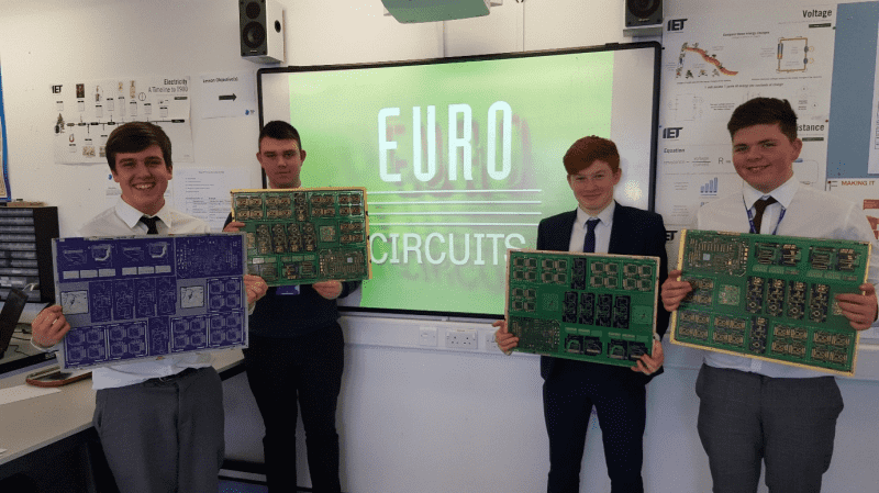
Wigan UTC students receive a Master class in PCB manufacturing from Eurocircuits
The 3rd of March 2016, Electronic engineering students at Wigan UTC were visited by Steve Jones, the Eurocircuits regional manager for UK and Ireland, based in Devon.
29 Apr 2016
-
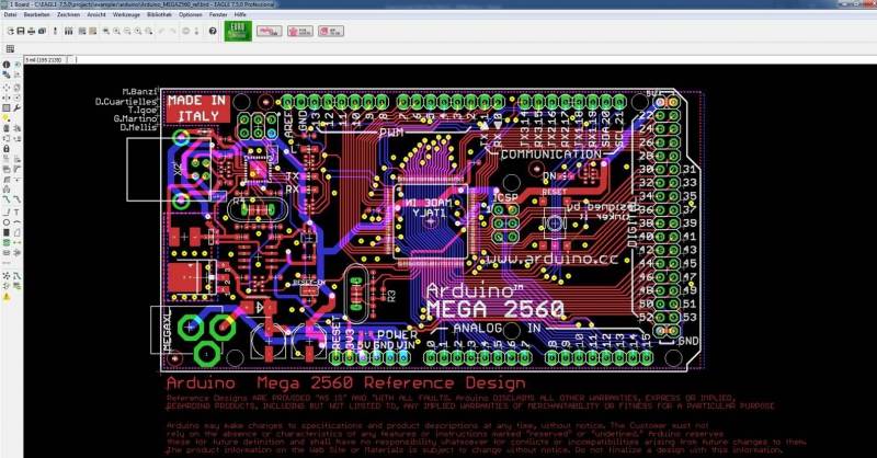
Eurocircuits ULP for EAGLE users
Eurocircuits ULP for EAGLE users - start calculating prices directly from your board parameters.
29 Apr 2016
-

eC-stencil-mate and eC-reflow-mate: what our users say
We now have more than 420 eC-stencil-mates and more than 450 eC-reflow-mates in use in the field. We have gathered together some comments from our users which we reproduce with their permission.
14 Jul 2015
-

Reflow soldering update: latest equipment, accessories
A complete solution from one supplier
14 Jul 2015
-
Eurocircuits Technical Update new pick and place unit unveiled
Eurocircuits unveil our latest equipment the eC-placer, camera-assisted manual pick and place to help realise your designs.
11 Jun 2015
-

SEMI-FLEX pool now available
Eurocircuits is proud to announce its latest service offering to electronics designers to provide cost effective solutions for prototyping and small series - SEMI-FLEX pool
11 May 2015
-
Eurocircuits release new NAKED proto service
When designing engineers need a cost effective Prototype board which can be easily modified to make there "Proof of concept" Naked proto is specifically designed with this in mind
11 May 2015
-

Eurocircuits involved in project that is out of this world: WUSAT-2
Eurocircuits had the immense pleasure to provide the PCBs for such a prestigious project as the recently launched WUSAT-2, and are very pleased to be sponsoring Warwick's next planned satellite
08 Apr 2015
-
The history of order pooling?
Order pooling is now a well-established technique used to cut costs for prototypes and small batch PCBs. But what is it and what is its history?
08 Apr 2015